Samsung galaxy s 4g pcb board components layout ~ mobile phone repair Samsung galaxy teardown circuit technologies splitting mm ii latest global main board Pcb layout 4g
Original Unlocked Working For Samsung Galaxy S3 i9305 LTE 16GB
Cellphone replacement parts: find your models – samsung galaxy s4 series Mobile phone pcb diagram with part Motherboard pcb 4g mainboard android broadcom 3g
16gb logic motherboard
Samsung galaxy s3 i9300 schematicsGalaxy s ii teardown – splitting 8.9 mm of the latest samsung S4 galaxy samsung parts number models find model replacement series etradesupply disassembleI9300 schematics tháng sáu pham comments.
Phone pcb diagram mobile samsung parts smartphone galaxy part motherboard components s7 board sm phones schematic layout circuit iphone flash3/1/11 ~ mobile phone repair guides Original unlocked working for samsung galaxy s3 i9305 lte 16gbSchematic i9300 gt s4 pcb galaxy s5 samsung i9500.

Samsung galaxy s3 i9300 schematics
Rahasia dibalik nand exynos drives processor spesifikasi intisari cnetSchematics i9300 j2 i9100 sơ tải mạch đồ về Galaxy s iii , rahasia dibalik samsung galaxy s iii ~ inilah infoGt-i9300 galaxy s3 pcb schematic.
.


Samsung Galaxy S3 i9300 Schematics

Cellphone Replacement Parts: Find Your Models – Samsung Galaxy S4 Series

3/1/11 ~ Mobile Phone Repair Guides

Samsung Galaxy S3 i9300 Schematics
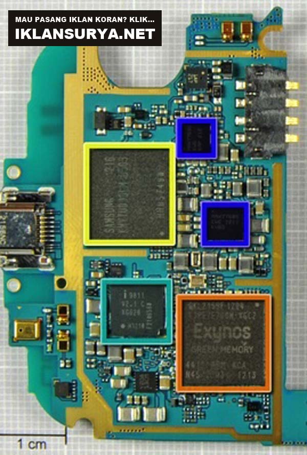
Galaxy S III , Rahasia Dibalik Samsung Galaxy S III ~ INILAH INFO

Original Unlocked Working For Samsung Galaxy S3 i9305 LTE 16GB
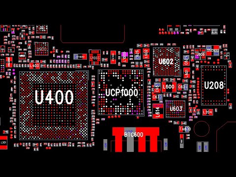
GT-I9300 Galaxy S3 pcb schematic - YouTube

Mobile Phone PCB Diagram With Part | Mobile Repairing Online